advanced devices
The Advanced Devices area focuses on the implementation of multifunctional structures, new generation micro / nanostructured devices with application in the fields of energy production, energy storage and energy saving.
CONTACT PERSONS
Vincenzo Maiorano, Luisa De Marco, Aurora Rizzo, Rosanna Mastria, Salvatore Gambino
KEYWORDS
Perovskite Solar Cell (PSC), Sustainable Batteries, Multifunctional devices for energy saving, Wearable Printed Electronics, Functional Materials, Electrical and Photoelectrical characterization
Specifically, the use of advanced bottom-up and top-down approaches allows to design and manufacture devices based on organic, inorganic and hybrid materials, on rigid and flexible substrates with innovative features compared to the state of art at high Technology Readiness Level (TRL).
These innovations in nanotechnologies, at the forefront of material science and advanced devices, are pivotal in designing and engineering eco-friendly hybrid organic/inorganic materials, as well as their precise implementation into micro/nanostructured active optoelectronic devices with low energy consumption.
The research lines of the Advanced Devices area are listed below:
Perovskite Solar Cells
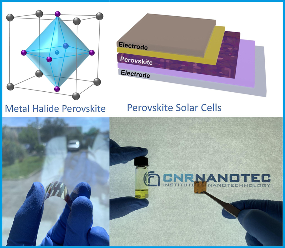
The latest generation photovoltaic cells based on hybrid halide perovskites have achieved in a few years, light conversion efficiency of over 26% exceeding the maximum efficiency currently achieved for thin film devices
Contact Persons
Aurora Rizzo
Keywords
Perovskite Solar Cell (PSC), Smart Windows
Wide bandgap and semitransparent solar cells are also developed to be integrated into tandem technology and into buildings as transparent photovoltaic windows. Fundamental in this context is the control of the growth conditions of the polycrystalline film in order to obtain high efficiency and stable devices. For the electrodes we study alternative materials to Indium Tin oxide (ITO) based on graphene.
People
Aurora Rizzo, Antonella Giuri, Rosanna Mastria, Silvia Colella, Nadir Vanni, Lucia Mercurio, Dawar Ali, Mario Calora, Liya Anthony, Sonia Carallo, Sara Covella, Vincenza Armenise, Andrea Listorti, Francesca Russo
Sustainable Batteries
Batteries are playing a key role in the clean energy transition, enabling the use of renewable sources and electric mobility. Currently, Lithium-ion Batteries (LiB) dominate the market but are based on critical raw materials (such as Cobalt), whose low natural abundance, high cost and toxicity urges the search for alternative materials.
Contact Persons
Luisa De Marco
Keywords
Organic batteries, Hybrid organic-inorganic nanostructured cathodes, Zn-air batteries, Biomass-derived materials
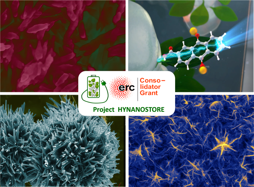
In the framework of the ERC Consolidator project ‘HYNANOSTORE’ we re-think the concept of battery’s electrode based on lithium insertion and develop new environment-friendly systems for energy storage based on organic redox materials, which can reversibly uptake and release electrons and cations (including Sodium or other cations), replacing critical raw materials. Organic redox materials are ubiquitous in nature or can be produced from biomass by green processes, therefore the battery can be produced from naturally abundant materials and at the end of its life can be easily recycled, so the environmental footprint of its life cycle is minimized, leading to a new generation of “green batteries”.
People
Luisa De Marco, Sabrina Di Masi, Francesco Biscaglia, Simone Bruno, Martina Scaramuzzo, Giuseppe Mianulli, Francesco Ruighi, Sonia Carallo
Multifunctional devices for energy saving
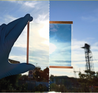
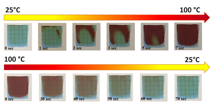
Chromogenic and multifunctional solid state devices are able to modulate the amount of solar radiation passing through them selectively and independently in the visible and infrared range through the application of an external stimulus (voltage, temperature, light) and using an appropriate active material, are included in the class of “green” nanotechnology for “Building Integration” and energy saving applications.
Contact Persons
Vincenzo Maiorano, Pierluigi Cossari
Keywords
Solid State Electrochromic (EC) Devices, Smart Windows, TADF
Combining the functionalities of energy production, lighting and controlled shielding, through the use of low consumption lighting sources (OLEDs, perovskite LEDs -PeLEDs), solid state chromogenic (dual-band electrochromic, thermocromic, photochromic) devices and organic and hybrid photovoltaic (PV) cells, “smart” and self-sustainable multifunctional devices can be implemented.
People
Vincenzo Maiorano, Fabrizio Mariano, Marco Pugliese, Antonio Maggiore, Sonia Carallo
Wearable electronics
Wearable optoelectronic devices have gained considerable interest in recent years due to their potential use in personal portable health monitoring, remote medical practices and improving safety conditions in the workplace.
Contact Persons
Vincenzo Maiorano
Keywords
Flexible optoelectronics, solution based electronics, large area production, chromogenic and light emitting fabrics, TADF
Thermally Activated Delayed Fluorescence (TADF) materials can be integrated into flexible or textile-based OLED displays, as well as into wearable optical sensors that can track multiple vital signs such as heart rate, blood pressure and oxygen levels. Other wearable applications include UV detection, measurement of pollutant levels and detection of explosives, both indoors and outdoors. Research activities focus on the realisation and characterisation of different types of optoelectronic devices on different substrates (e.g. fabrics) and their combination with other components to realise flexible, easily processable smart systems with enhanced functionalities. Thermochromic, photochromic and electrochromic systems have also been developed using innovative organic (carbon-based) semiconductors, hybrid systems incorporating both organic and inorganic materials (3D-2D perovskites), nanoparticle-based inks (e.g. colloidal 2D-TMDC, carbon nanotubes, graphene), processed by wet techniques (printing and coating methods) for large area production.
People
Vincenzo Maiorano, Fabrizio Mariano, Marco Pugliese, Antonio Maggiore, Sonia Carallo

Materials for optoelectronic and photonic devices
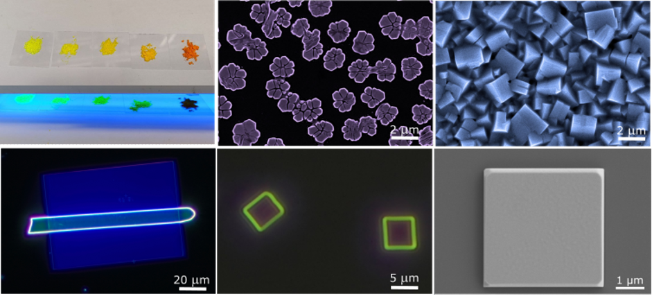
Metal halide perovskites have demonstrated remarkable opto-electronic properties in recent years, including a high coefficient of light absorption, high oscillator strength, efficient ambipolar charge transport, high defect tolerance, and simple solution-based preparation.
Contact Persons
Rosanna Mastria, Aurora Rizzo, Luisa De Marco
Keywords
Perovskites engineering, Perovskite nanocomposites, Perovskite single-crystals
These characteristics make them ideal for a wide range of applications, such as photovoltaics, light-emitting diodes, and ionizing radiation detectors. Our research focuses on understanding the fundamental properties of these materials and investigating their operating mechanisms within various types of devices. We also explore several material development strategies to engineer the composition, optical and electronic properties of perovskites to meet specific device requirements. The materials developed in our laboratories range from hybrid (organic-inorganic) perovskites to completely inorganic perovskites with different dimensionalities (2D and 3D).
People
Rosanna Mastria, Aurora Rizzo, Luisa De Marco, Ilenia Viola, Mario Calora, Amal Chandran Chekkallur, Simone Bruno, Francesco Saverio Difeo, Sonia Carallo, Pierluigi Cossari
Electrical and Photoelectrical Characterization of Optoelectronic Devices
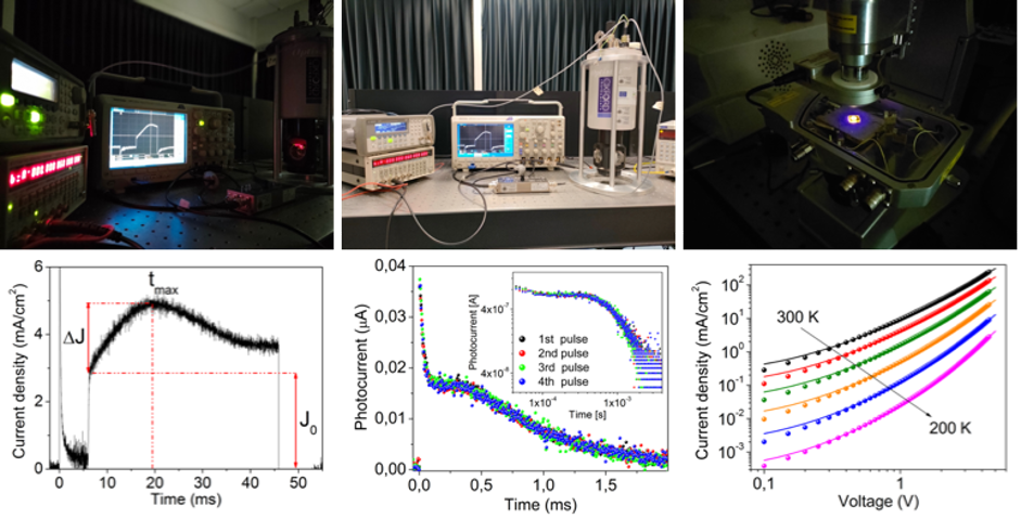
A range of material properties can be extracted from photo-electrical experiments, such as charge generation and recombination, mobility, doping and charge trapping mechanisms, injection properties of the contacts and eventually ionic contribution.
Contact Persons
Salvatore Gambino
Keywords
Electro-Optical Characterization, Charge Transport, Mobility, Time of Flight (TOF), Charge Extraction by Linearly Increasing Voltage (CELIV), Thermally Stimulated Current (TSC), Space Charge Limited Current (SCLC)
As these parameters are entangled, only the combination of different measurement techniques that combine steady-state, transient, and frequency-domain experiments can give a reliable insight into device physics. We have developed different photoelectrical characterization techniques that can be used on organic, inorganic and hybrid semiconductors or into operationally working devices.
DC Measurements
With direct-current (DC) measurements we refer to the electrical steady-state characterization of semiconductors and devices. The measurement can be carried out with the device in dark conditions or under various illumination intensities, under controlled environmental conditions and temperatures.
-
- Current-Voltage (J-V) and JV-Luminescence (J-V-L) measurements
- 4-point probes resistivity measurements and Hall mobilities
Transient Measurements
The measurement of a transient entails the recording of the response of an electrical parameter (like current or voltage) over time after the application of a stress. The stress can be illumination, voltage bias, or a combination of the two.
-
- Charge Extraction by Linearly Increasing Voltage (CELIV)
- Time of Flight (TOF)
- Thermally Stimulated Current (TSC)
People
Salvatore Gambino, Adriano Cola
